Photo Credit: Kai Fu – Wu Lab, Princeton University
Quasiparticle-assisted Electrothermal feedback TES (QET)
G4CMP is primarily used for simulations in the material of a detector crystal, but it also supports some methods and classes for simulating detector response to events within the crystal. The following serves as a summary and applications of the physics G4CMP uses for modeling energy transport in QETs.
Kaplan Quasiparticle Model
This model is used for thin-film superconductors common in cryogenic electronic sensors, such as TESs or QETs, KIDs, and qubits. These sensors are populated with Cooper pairs, which can be broken upon phonon absorption into electron quasiparticles. For small films, quasiparticles
transport faster than the thermal response. As for Crystal properties, aluminum film parameters are supplied with the package via a Geant4 properties table, including film thickness, Cooper pair gap energy (2Δ), vsound, and phonon lifetime.
G4CMP models energy transfer, QP transport, and phonon re-emission via the G4CMPKaplanQP class.

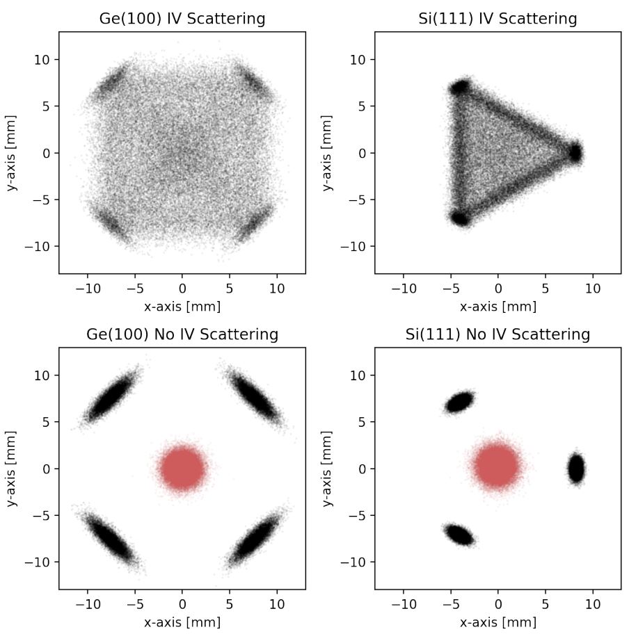
G4CMP simulations of electron transport (black) through 1.67 cm thick Ge (left) and Si (right) crystals, both with (top) and without (bottom) intervalley
(IV) scattering. In the former case (top), intervalley scattering tends to scatter electrons toward the center of the crystal and thus encourages transport to align with the applied field. For the cases without intervalley scattering (bottom), hole transport is also shown and appears as central clusters (red). The 0.5 V/cm electric field is applied along the z axis, which aligns with the h100i crystal axis in the case of Ge and the h111i axis for Si.
G4CMPKaplanQP
In G4CMPKaplanQP, the simulation of the Kaplan Quasiparticle Model is treated as instantaneous; it iterates to find the equilibrium state and contains no time-dependent information.
Substrate phonon absorption in the thin film is modeled by using the mean free path and thickness to find the probability of this occurring. In particular,
where P is the probability of substrate phonon absorption, d is the film thickness, MFP is the mean free path, and 𝛕 is the phonon lifetime.
Phonon energy in these simulations goes to break Cooper pairs, and becomes the QP energy. QP or phonon energy is absorbed into the tungsten TES, at which time some QP energy goes back into phonons via QP “decay” (emission), and some phonon energy is re-emitted back into the substrate. In G4CMPKaplanQP, the processing loop ends when the available phonon energy is zero. This model is not suitable for “bare” films that lack an attached energy absorber.

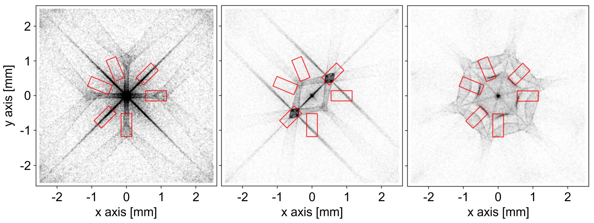
Patterns of phonon caustics simulated using G4CMP for a 5 × 5 mm2 , 350 µm thick silicon chip cut at different crystal orientations: (from left to right) <100>, <110>, <111> orientations. The red rectangles indicate proposed positions of sensors to collect phonon energy.
Phonon Readout Model
Phonon energy deposits are collected in time bins resulting in a matching readout. Coupled differential equations model the electrothermal response of TESes, the bias current, indicative (SQUID) coupling, and other phenomena. CVODE (from LLNL) is used to solve for current output in each time bin, while configuration files specify detector components and characteristics including heat flow, resistances, inductances, TESes per channel, and others.